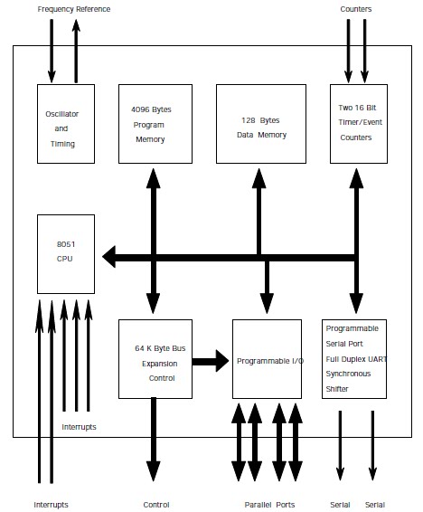


The architecture of the 8051 family of microcontrollers is referred to as the MCS-51
architecture, or sometimes simply as MCS-51. The microcontrollers have an 8-bit
data bus. They are capable of addressing 64K of program memory and a separate
64K of data memory. The 8051 has 4K of code memory implemented as on-chip
Read Only Memory (ROM). The 8051 has 128 bytes of internal Random Access
Memory (RAM). The 8051 has two timer/counters, a serial port, 4 general purpose
parallel input/output ports, and interrupt control logic with five sources of interrupts.
Besides internal RAM, the 8051 has various Special Function Registers (SFR), which
are the control and data registers for on-chip facilities. The SFRs also include the
accumulator, the B register, and the Program Status Word (PSW), which contains the
CPU flags. Programming the various internal hardware facilities of the 8051 is
achieved by placing the appropriate control words into the corresponding SFRs. The
8031 is similar to the 8051, except it lacks the on-chip ROM.
As stated, the 8051 can address 64K of external data memory and 64K of external
program memory. These may be separate blocks of memory, so that up to 128K of
memory can be attached to the microcontroller. Separate blocks of code and data
memory are referred to as the Harvard architecture. The 8051 has two separate read
signals, RD# (P3.7) and PSEN#. The first is activated when a byte is to be read from
external data memory, the other, from external program memory. Both of these
signals are so-called active low signals. That is, they are cleared to logic level 0 when activated.
All external code is fetched from external program memory. In addition,
bytes from external program memory may be read by special read instructions such
as the MOVC instruction. There are separate instructions to read from external data
memory, such as the MOVX instruction. That is, the instructions determine which
block of memory is addressed, and the corresponding control signal, either RD# or
PSEN# is activated during the memory read cycle. A single block of memory may be
mapped to act as both data and program memory. This is referred to as the Von
Neumann1 architecture. In order to read from the same block using either the RD#
signal or the PSEN# signal, the two signals are combined with a logic AND operation.
This way, the output of the AND gate is low when either input is low. The advantage
of the Harvard architecture is not simply doubling the memory capacity of the
microcontroller. Separating program and data increases the reliability of the
microcontroller, since there are no instructions to write to the program memory. A
ROM device is ideally suited to serve as program memory. The Harvard architecture
is somewhat awkward in evaluation systems, where code needs to be loaded into
program memory. By adopting the Von Neumann architecture, code may be written
to memory as data bytes, and then executed as program instructions.
The 8052 has 256 bytes of internal RAM and 8K of internal code ROM. The 8051 and
8052 internal ROM cannot be programmed by the user. The user must supply the
program to the manufacturer, and the manufacturer programs the microcontrollers
during production. Due to the setup costs, the factory masked ROM option is not
economical for small quantity productions. The 8751 and 8752 are the Erasable
Programmable Read Only Memory (EPROM) versions of the 8051 and 8052. Many
manufacturers offer the EPROM versions in windowed ceramic and non-windowed
plastic packages. These are user programmable. However, the non-windowed
versions cannot be erased. These are usually referred to as One-Time-
Programmable (OTP) microcontrollers, which are more suitable for experimental work
or for small production runs. The 8951 and 8952 contain FLASH EEPROMs
(Electrically Erasable Programmable Read Only Memory). These chips can be
programmed as the EPROM versions, using a chip programmer. Moreover, the
memory may be erased. Similar to EPROMs, Erasing FLASH memory sets all data
bits (data bytes become FFh). A bit may be cleared (made 0) by programming.
However, a zero bit may not be programmed to a one. This requires erasing the chip.
Some larger FLASH memories are organized in banks or sectors. Rather than
erasing the entire chip, you may erase a given sector and keep the remaining sectors
unchanged.
During the past decade, many manufacturers introduced enhanced members of the
8051 microcontroller. The enhancements include more memory, more ports, analogto-
digital converters, more timers with compare, reload and capture facilities, more
interrupt sources, higher precision multiply and divide units, idle and power down
mode support, watchdog timers, and network communication subsystems. All
microcontroller of the family use the same set of machine instructions, the MCS-51.
The enhanced features are programmed and controlled by additional SFRs. In the
remainder of this chapter, the hardware architecture of the 8051 is presented. The
enhancements brought by the 8052 and 80C515 follow. Some of the more popular
enhanced members of the family are reviewed at the end of Chapter 2. The reader is
referred to the manufacturers' data books for the specifics of other enhanced
members.
No comments:
Post a Comment